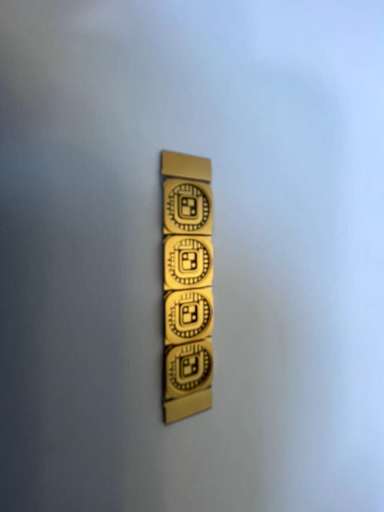
Embedded Cavity PCB Substrate Manufacturer.Embedded Cavity PCB Substrate Manufacturer, and step cavity PCB substrates production from 4 layer to 30 layers. the PCB will be made with High frequency and high speed PCB materials.
Embedded cavity PCB substrate is an advanced technology aimed at enhancing circuit performance and reliability through the integration of a cavity structure within the substrate. This innovative approach is pivotal in electronic device design, offering novel solutions across diverse application contexts.
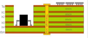
In traditional PCB design, the components on the circuit board are usually surface mounted, but embedded cavity PCB substrates take a different approach. It creates a cavity or space inside the substrate so that circuit components can be installed in a more hidden position, thereby achieving a more compact design and higher integration.
This design provides multiple benefits. Firstly, the built-in cavity enhances EMI/RFI shielding, minimizing the effects of electromagnetic interference on the circuitry. Secondly, it enhances heat dissipation, thereby maintaining stable temperature levels for the circuit components. Additionally, the cavity serves to protect components from physical harm and environmental influences.
Embedded cavity PCB substrates find extensive application in electronic devices such as smartphones, tablets, computers, communication equipment, as well as various industrial and automotive electronics. They enable designers to create smaller, lighter, and higher-performing products while enhancing stability and reliability.
Embedded cavity PCB substrates are a cutting-edge technological integration that expands the horizons of circuit design. They boost the performance and dependability of electronic devices while offering designers increased creative freedom and potential for innovation. As technology evolves, embedded cavity PCB substrates will remain instrumental in advancing and shaping the electronics industry.
What are the advantages of embedded cavity PCB substrate?
Embedded cavity PCB substrates are an innovative technology gaining popularity, especially in high-tech applications. They offer several advantages over traditional PCB substrates. Firstly, they achieve higher circuit integration by incorporating a cavity structure, enabling more electronic components to fit in a smaller space, thus enhancing circuit performance and efficiency. Secondly, these substrates demonstrate superior heat dissipation capabilities through the cavity structure, efficiently transferring heat from electronic components to dissipate it through the substrate, thereby enhancing equipment stability and reliability. Additionally, they feature smaller dimensions due to the compact layout facilitated by the cavity design, making electronic devices lighter and more portable, aligning with modern trends favoring slim and lightweight products. Moreover, their design flexibility is unparalleled, allowing for intricate and precise circuit layouts, meeting diverse application needs in fields like communication, medicine, and aerospace. In essence, embedded cavity PCB substrates are the preferred choice in high-tech realms, offering advantages such as high integration, excellent heat dissipation, compact size, and versatile design capabilities, poised to play an increasingly pivotal role in the future as technology advances and application domains expand.

Embedded Cavity PCB Substrate
Why choose embedded cavity PCB substrate?
In today’s electronic engineering world, choosing the appropriate PCB substrate is crucial. Among the many options, why choose embedded cavity PCB substrate? What exactly are its advantages in a specific project?
Improving Performance and Reliability: The embedded cavity PCB substrate design is focused on creating an internal cavity structure. This approach enhances circuit performance and reliability by optimizing layout and reducing signal and electromagnetic interference.
Increased Integration: Embedded cavity PCB substrates enable higher integration, packing more functions and components into a smaller space. This compact design reduces equipment size and enhances system performance and efficiency.
Tailored to Specific Scenarios: Embedded cavity PCB substrates are well-suited for projects with demanding space and performance requirements. Their compact design and superior performance make them ideal for portable devices or embedded systems.
Customizable Flexibility: Manufacturers can customize embedded cavity PCB substrates to meet specific project needs, ensuring optimal performance and functionality.
In summary, embedded cavity PCB substrates are chosen not only for their technical advantages but also for their ability to meet project-specific requirements for performance, size, and reliability. In modern electronic engineering, they are increasingly becoming the preferred choice across various application scenarios.
How is the embedded cavity PCB substrate made?
The manufacturing process of embedded cavity PCB substrates is intricate and demands precision, blending advanced technology with skilled craftsmanship. It commences with the design phase, where engineers utilize computer-aided design (CAD) software to outline the substrate’s layout, connections, and cavity structure. Factors like circuit functionality, board thickness, interlayer connections, and cavity dimensions are carefully considered during this phase.
Material selection stands out as a pivotal stage in the manufacturing journey. Common substrate materials encompass FR-4 fiberglass composite materials alongside specialized options such as PTFE (polytetrafluoroethylene). In the context of embedded cavity PCB substrates, material choice hinges on meeting performance demands in high-frequency and high-temperature environments, among other considerations.
Next comes the step of machining the cavity. This is usually done by machining or laser processing. In this process, engineers create cavity structures inside the substrate to accommodate specific components or circuits based on design requirements.
After finishing the cavity, the next steps are lamination and stacking. At this stage, engineers stack the individual layers of the multilayer substrate together and use heat-pressing technology to hold them together. This ensures the board’s robustness and reliability.
Before laminating the substrate’s interior, the initial step involves generating the inner circuit pattern. This process entails transferring the circuit pattern onto the inner layer of the substrate, commonly achieved through techniques like photolithography or laser cutting.
Upon completion of the inner circuit pattern, engineers proceed to create the circuit pattern on the substrate’s surface. This typically involves etching the desired pattern of wires and connectors onto the substrate’s surface, utilizing techniques such as chemical etching or laser etching.
Through these crucial steps and technologies, the manufacturing of embedded cavity PCB substrates is accomplished. This precision manufacturing process ensures the substrate’s performance and reliability, allowing it to play a vital role in various high-end applications.
In what fields are embedded cavity PCB substrates used?
Embedded cavity PCB substrate is a technological innovation that is showing great application potential in multiple electronic equipment fields. Its wide application in fields such as smartphones, computers and communication equipment is changing the pattern and development trends of these industries.
In the design and manufacturing of smartphones, embedded cavity PCB substrates play a key role. As smartphones have increasing requirements for size, performance and heat dissipation, the high degree of integration and superior heat dissipation performance of embedded cavity PCB substrates make them the first choice. Through embedded cavity PCB substrates, smartphones can achieve more efficient circuit layout, improve performance, and accommodate more functional components in a smaller volume.
In the field of computer hardware, especially in high-performance computers and servers, embedded cavity PCB substrates also play an important role. These application scenarios require circuit boards with higher density and faster data transmission speeds to meet the requirements of complex computing tasks. By using embedded cavity PCB substrates, computer systems can achieve higher performance and reliability while reducing failure rates and energy consumption.
Embedded cavity PCB substrates are gaining popularity in communication equipment, spanning from base stations to network routers, communication satellites, and wireless access points. These devices demand stringent circuit board requirements, and embedded cavity PCB substrates meet these demands by offering higher integration, improved signal transmission, enhanced anti-interference capabilities, and heightened device stability and reliability. Their increasing application in smartphones, computers, and various communication equipment sectors signifies a deepening integration, driving further development and innovation in these industries. With their exceptional integration, performance, and reliability, embedded cavity PCB substrates stand out as a pivotal technology in contemporary electronic engineering.

Embedded Cavity PCB Substrate
Where are the manufacturers of embedded cavity PCB substrates?
Manufacturers of embedded cavity PCB substrates are crucial, but how to find a reliable manufacturer? Which manufacturers are trustworthy in this rapidly growing field? We’ll dive into these questions and provide some guidance on finding a manufacturer.
First of all, to find a reliable embedded cavity PCB substrate manufacturer, you can go through the following ways:
To find embedded cavity PCB substrate manufacturers, consider utilizing online searches, attending industry trade shows and conferences, engaging in industry forums, and relying on references and word-of-mouth. Online searches can yield manufacturer websites and directories, while trade shows offer direct communication opportunities with manufacturers. Industry forums facilitate sharing experiences and seeking recommendations. Additionally, checking customer reviews and reputation aids in selecting reliable manufacturers.
What is the price of embedded cavity PCB substrate?
To ascertain the price of embedded cavity PCB substrates, requesting a quote is the initial step. However, their pricing is influenced not only by manufacturing expenses but also by market dynamics and other pertinent factors.
First of all, to get an accurate embedded cavity PCB substrate price, it is best to contact a reliable manufacturer or supplier directly. These professional companies will provide corresponding quotations based on the specific needs of customers, including board size, number of layers, materials and other factors. Additionally, prices may vary if there are custom needs or special requests.
Market pricing is a crucial determinant of embedded cavity PCB substrate costs, influenced by various factors such as competition among numerous manufacturers and suppliers, as well as market dynamics like supply and demand, industry trends, and competitor pricing. Additionally, fluctuations in raw material prices, advancements in manufacturing processes, and technological innovations contribute to fluctuations in product costs, thereby impacting prices indirectly. Overall, the price of embedded cavity PCB substrates is the culmination of multiple considerations, necessitating consultation with professional manufacturers or suppliers for accurate quotes. Vigilance towards market dynamics and related factors is also essential for making well-informed decisions.
What are the common problems with embedded cavity PCB substrates?
What are embedded cavity PCB substrates?
Embedded cavity PCB substrates are advanced circuit boards designed with internal cavities to enhance performance and reliability. These substrates play a crucial role in various electronic devices, offering superior thermal management and miniaturization capabilities.
What are the common challenges associated with embedded cavity PCB substrates?
Common challenges associated with embedded cavity PCB substrates include design complexity, manufacturing tolerances, and thermal management. Proper design consideration and collaboration with experienced manufacturers can help mitigate these challenges and ensure successful implementation of embedded cavity PCB substrates in electronic systems.
Where can I find reputable manufacturers of Embedded Cavity PCB Substrates?
Finding reliable manufacturers is crucial. Look for experienced manufacturers with advanced production techniques. The keyword “Embedded Cavity PCB Substrate Manufacturer” can guide you to exceptional manufacturers in this field.
What advantages does an Embedded Cavity PCB Substrate offer?
Embedded Cavity PCB Substrates provide several advantages over traditional PCBs. These include higher integration, smaller form factor, and superior heat dissipation. Discover why they are considered the preferred choice in high-tech applications.
Why choose an Embedded Cavity PCB Substrate over other options?
Learn why Embedded Cavity PCB Substrates stand out among various PCB options. Explore the specific advantages that make them the ideal choice for certain projects.
How is the manufacturing process of Embedded Cavity PCB Substrates conducted?
Understand the intricate manufacturing process of Embedded Cavity PCB Substrates, covering key steps in producing both the main and bottom boards. Explore the associated technologies and processes involved.
In which fields are Embedded Cavity PCB Substrates widely applied?
Discover the extensive applications of Embedded Cavity PCB Substrates in various electronic devices such as smartphones, computers, and communication equipment. Gain insights into their significance in practical projects.
Where can I find suitable Embedded Cavity PCB Substrates for my needs?
Obtain guidance on finding Embedded Cavity PCB Substrates that meet your specific requirements. Get recommendations on suppliers and manufacturers to ensure you make an informed decision.
